
Put the RF reference plane first.
Define core and bondply, dielectric spacing, finished copper and the return path for each controlled-impedance layer.
Plan the cross-section →RF materials / design / fabrication
Understand the laminate. Resolve the geometry. Define a board that can be manufactured and measured.
Material properties, practical design tools and fabrication guidance for your next RF project.
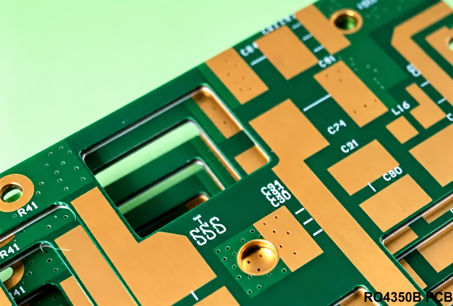
01 / Know the material
RO4350B is a glass-reinforced hydrocarbon ceramic laminate used in RF and microwave printed circuits. Its electrical properties and processing characteristics make it a candidate for controlled-impedance designs where conventional FR-4 needs closer evaluation.
Process Dk is a material test result. Design Dk is a modeling reference. Select the value that matches your structure, frequency and fabrication data rather than treating the two as interchangeable.
Explore the material guide →| Property | Reference |
|---|---|
| Process dielectric constant | 3.48 ± 0.05 at 10 GHz |
| Typical design dielectric constant | 3.66 |
| Dissipation factor | 0.0037 at 10 GHz |
| Thermal conductivity | 0.69 W/(m·K) |
Source: RO4000 laminate data sheet. The 4 mil construction has a separate process Dk of 3.33 ± 0.05. Design Dk uses a different method over 8–40 GHz. Typical values are not finished-board acceptance limits. Confirm the current material revision for procurement.
02 / Work through the geometry
Explore how conductor width and dielectric height affect microstrip impedance. Use the result to prepare a stackup discussion, then validate the final geometry with a field solver and your fabricator.
A quasi-static, zero-thickness microstrip approximation with a continuous ground plane and an air region above the trace.
Copper thickness and roughness, etch shape, solder mask, frequency dispersion, nearby conductors and finished dielectric thickness.
Read calculation assumptions →03 / Specify the build
Define core and bondply, dielectric spacing, finished copper and the return path for each controlled-impedance layer.
Plan the cross-section →Agree etch compensation, drilling, plating, registration and surface finish before releasing production files.
Review fabrication inputs →Specify the applicable IPC documents, revision, class, impedance coupons and inspection records for the project.
Build an acceptance plan →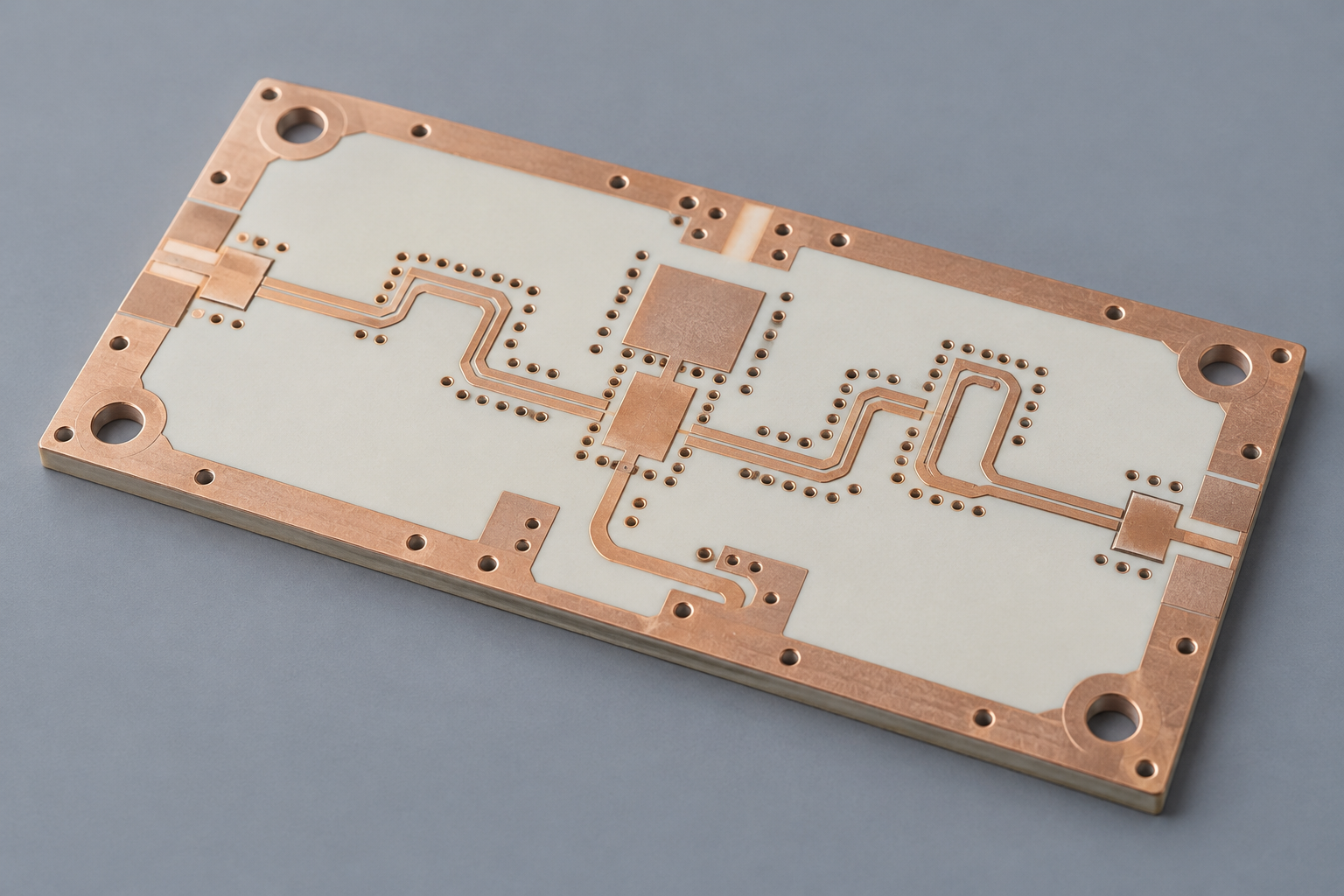
04 / Manufacturing workflow
Resolve drawing, drill, netlist and stackup discrepancies.
Agree material grades, copper, finish and controlled geometry.
Connect tolerances to electrical tests and inspection records.
Keep the approved manufacturing package and changes traceable.
05 / Application engineering
Evaluate RO4350B against your loss budget, thermal path, frequency range and assembly requirements.
Explore application considerations →Inspect phase balance, feed loss, connector launches and dimensional tolerances. Validate radiation performance on the finished assembly.
Check coupling gaps, line widths, surface finish and enclosure effects. Small geometric changes can shift the response.
Develop the thermal path independently of the RF match. Laminate thermal conductivity alone does not establish power-handling capability.
Design the calibration reference planes and de-embedding structures alongside the device interface.
Engineering reading
Compare additional RO4350B PCB fabrication considerations and review high-frequency laminate manufacturing options when preparing your project requirements.
Separate laminate loss tangent from PCB insertion loss, define reference planes, and plan the simulation and test evidence for an RF loss budget.
Choose the right RO4350B dielectric input, compare circuit models, and define coupons and fabrication records that verify the finished structure.